
Subscribe now and get the latest blog posts delivered straight to your inbox.
This article was originally published on August 9, 2021, and was updated on June 5, 2023.
The semiconductor industry affects nearly every aspect of our lives today. Your cell phone, computer, television, car and any other electronic device you use each day all depend on semiconductor applications to exist. But these demanding applications require specialized high-purity equipment and instruments to run safely, efficiently and properly.
Pressure transducers (and pressure transmitters but for simplification in this article I will refer to them as "pressure transducers") are crucial to the semiconductor process, but only if they are manufactured a certain way to handle hazardous environments. How do you know what makes the best semiconductor pressure transducer?
In this article, I will discuss what is involved in the semiconductor application process and what makes the best semiconductor pressure transducer to use in these processes so you can find the proper equipment for your application.
The Semiconductor Process
As you may be familiar with by now, the semiconductor process involves the highly complex transformation of a blank silicon wafer into discrete microelectronic devices. A circuit design and pattern are developed, which are then etched onto the wafer.
The wafers can then be broken into individual circuits to be used in electronic devices. This production process must take place inside a high-purity cleanroom environment to prevent any debris from damaging the circuits.
The global semiconductor industry is expected to continue robust growth over the next few years, so semiconductor suppliers face the challenge of improving supply to meet demand, especially for materials in emerging technologies such as artificial intelligence (AI), autonomous driving, the Internet of Things (IoT) and 5G—i.e., increasing transistor density, improving reliability, and reducing production and purchasing costs.
Many applications need the semiconductor process, including CVD (Chemical Vapor Deposition, or using a carrier gas to dilute toxic gas), photolithography, dry etching, wet etching and wafer cleaning. But the pressure instrumentation used needs to be of a certain quality to handle these delicate environments.
The equipment and instruments used in these processes must be manufactured a certain way, so let’s discuss the type of pressure transducer that is needed for the semiconductor industry.
Critical Factors for Pressure Transducers in Semiconductor Applications
There are many factors that make a pressure transducer appropriate for a hazardous semiconductor process:
Contamination Control
To reduce costs and increase performance, semiconductor manufacturing is continually challenged to increase the amount and density of the circuitry that can fit into each wafer. This is accomplished by constantly shrinking the features and patterns on the wafer itself, which is often called minimum feature size and measured in nanometers (nm).
In the early 1990s, this minimum feature size was 350 nm (approximately 1/250th the width of a human hair). In 2021, the finest processes have shrunk to as small as 5 nm!
To continue making circuit patterns smaller and smaller, extensive contamination control is necessary during the semiconductor process to avoid even the smallest foreign particles from creating defects and damage to the exposed wafer surfaces.
Smooth Surfaces
Pressure transducers that measure and control the ultra-high purity gases used in the semiconductor process must be purpose-designed to not introduce or trap foreign particles inside their cavities. The portion of the pressure transducers exposed to the UHP gases must be extensively cleaned and have a shiny, smooth service.
Smooth surfaces reduce the surface area exposed to the process and result in less chance of moisture or foreign particles sticking to the service of the instrument during installation and after repeated use.
High-Quality Material
The material used in the construction of pressure transducers must be compatible with the process media and be of extremely high quality. High purity grades of 316L stainless steel are most commonly utilized for pressure transducers due to their high resistance to corrosion as well as their resistance to hydrogen embrittlement, which can impact the long-term safety, repeatability and stability of pressure transducers.
Safety Approvals
Also, semiconductor gases can be flammable, toxic and explosive, so careful selection of a pressure transducer with appropriate approvals for intrinsic safety or non-incendive locations must be made to address critical safety concerns.
We don’t like to pressure you, but we have more information.
Now that you understand more about the demands of semiconductor applications on your pressure instruments, you should be prepared to shop. These processes require high-purity clean instruments and the utmost care to ensure the materials are not damaged.
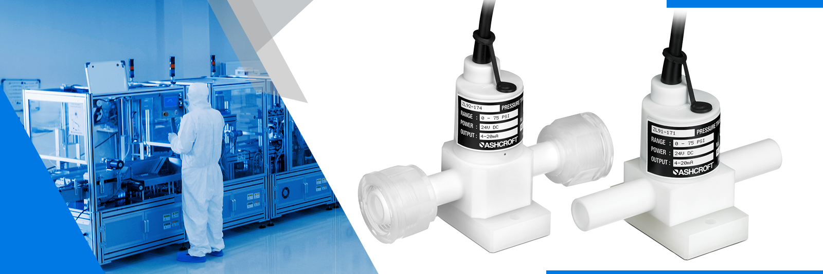
Ashcroft offers the ZT12 and ZX12 series pressure transducers for the semiconductor industry. The gas contact surfaces are all made of 316L stainless steel and electro-polished to minimize surface area and help eliminate impurities inside the process.
These products are compatible with numerous process gasses and demonstrate extremely high stability for long-term process measurement. The ZX12 features ATEX and IECEX location approvals for hazardous areas.
Ashcroft’s parent company Nagano Keiki manufactures pressure sensors using these semiconductor processes in-house, which is its busiest industry. Nagano Keiki has sold their ultra-high purity products for over 30 years making them experts in what customers in the semiconductor industry need.
If you want to learn more about pressure transducers, feel free to visit our website and view any of our product pages, or helpful blog articles, guides or webinars in our resource center.
At Ashcroft, we are committed to helping customers select and source the right instruments for their needs. Whether you need assistance choosing instruments for a new process or operation, or if you need something custom-built for your specific application, we’ve got you covered.
Reach out today to talk to one of our industry experts and get your questions answered. Or take a look at our guide:


